High-Resolution Scanning Electron Microscopy and Microanalysis
Textural properties of ores and other materials typically feature microscopic, sometimes nanoscopic, attributes. Hence, detailed materials and ore characterization, metallurgical testing, and mineral processing are prime uses for the imaging and analysis tool.
FEATURES
A scanning electron microscope (SEM) produces images of a sample by scanning it with a focused beam of electrons. The electrons interact with atoms in the sample, producing various signals that contain information about the sample's surface topography and composition with a magnification range that encompasses that of optical microscopy and extends it to the nanoscale.
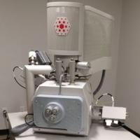
The FEI Quanta 650F SEM is equipped with a large specimen chamber, two Bruker XFlash 6-series high-speed energy dispersive x-ray spectrometers (EDS), and automated quantitative image analysis and microanalysis software.

Dust-Coated Fibers
Main image horizontal field width (HFW) is 1.58 mm; inset HFW is 109 µm.
 Particulates on Filter Membrane
Membrane aperture size is 0.02 µm (20 nanometers).

Complex Particle in Zinc Rougher Concentrate (sphalerite, galena, and mica)
Main image HFW is 265 µm; inset HFW is 69.5 µm.

Resolution Standard (gold on carbon substrate)
Service Applications
Related Capabilities
Contact Hazen
Main (303) 279 4501
Fax (303) 278 1528
E-mail / Directions
Submit RFP